Big Changes to ESP32 effort

Over the summer, what with the rainy New England weather this year, I spent quite a bit of time on the ESP82 prototype. Those that follow this blog know that I’ve been teasing an ESP32 version for a couple of years now, and although I have had a pretty good working prototype for about that long, several developments caused me to question major parts of it.

It all started when I could no longer get the AC reference transformers that I’ve been selling for a couple of years. That, coupled with all the ZMPT101B craze in the IOT world, and a little inspiration from recently release OEM power supply that uses it, got me to evaluating the feasibility of integrating one or three of them directly into the IoTaWatt PCB.

Unfortunately, I could not get the thing to work as accurately as I would like across a wide voltage spectrum (100V-277V). While the ratio of input current to output current is fairly steady, my experience is that the power consumed by the sample resister shown up as additional source current, and so the calibration is not a simple gain+offset calculation. Moreover, I found unacceptable variance between the ten samples that I got.

After spending quite a lot of time on redesigning the sampler to use three onboard voltage sensors, I could not revert to a simpler design. So, I started to look for something better. I believe I found it.

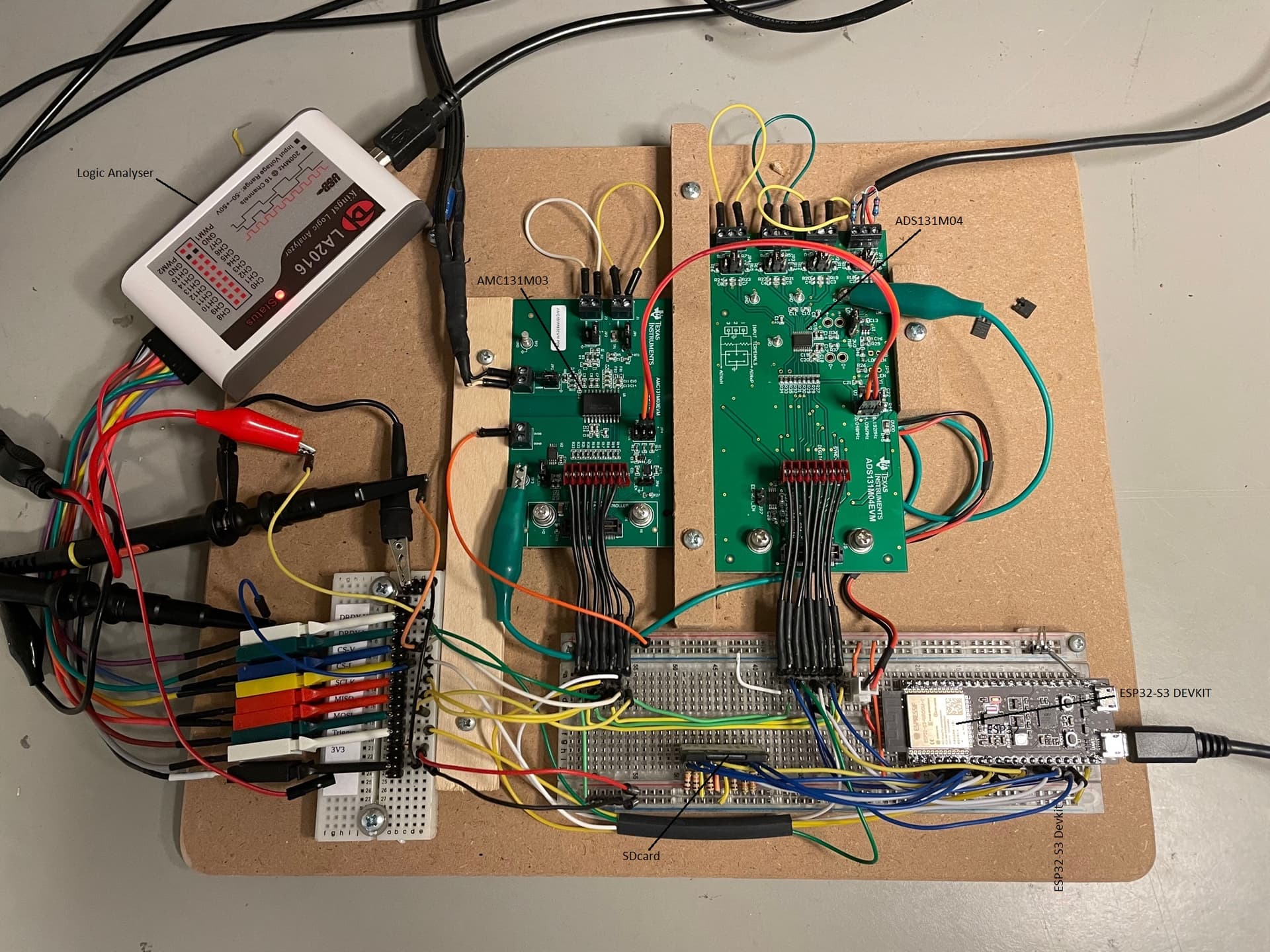
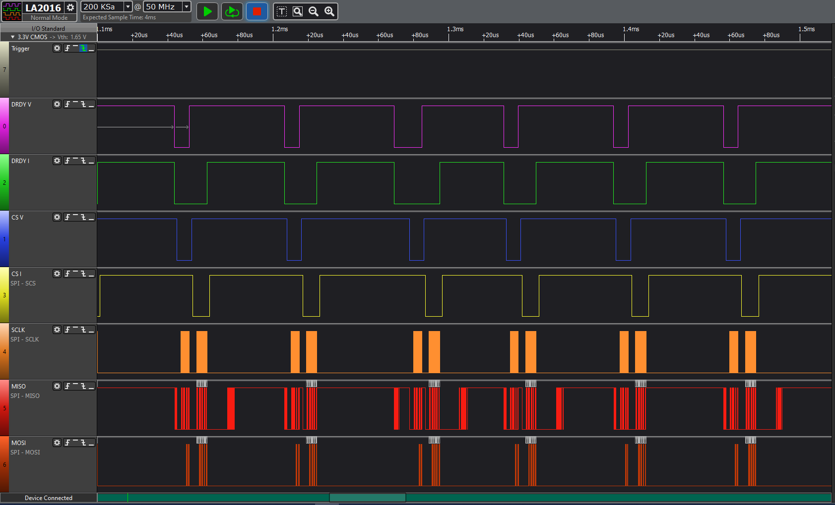
Texas Instruments has a new chip, the AMC131M03. This chip provides reinforced isolation of the analog side and sports three 24 bit Sigma-Delta ADCs. Moreover, it will sample all three voltages simultaneously and continuously. The chip is a variation of the ADS131Mnn family of 24 bit Sigma-Delta ADC chips that can have up to 8 simultaneous differential inputs.

So a few weeks ago, I got some evaluation kits for these things. I find that I can sample voltage directly with about 0.1% accuracy. On the current side, the ADS132Mnn chip takes a differential input from the CTs, obviating the need for any bias voltage and completely isolating each CT from the others.

All of the ADCs would sample at the same time (Oh, except for slight timing offsets to compensate for CT phase shift), and the ESP32 appears fast enough to read the voltages and as many as 32 CT inputs at 16K samples/second. Very exciting.

These chips are pretty much designed for use in high accuracy electric meters. Cost is higher than the MCP3208 ADCs used in the old design, and more are needed, but it’s not prohibitive given the accuracy possible.

While I was at it, I have upgraded from using the ESP32 WROVER to the newer ESP32S3 which offers a lot more resources. I believe Ethernet will be possible as well.

All of the back-end improvements remain the same with the datalog, web-server, and query subsystems. With the continuous sampling, one second resolution data should be highly accurate and so possibly an MQTT stream will be added.

With much reduced time spent selling the 8266 units, I’m really enjoying getting back to R&D. I’ll post more as I get these ADCs working in the prototype.

18 Likes

Sounds like some very promising enhancements! Thank you for sharing the update. Looking forward to seeing some comparison data between the existing ESP8266 platform and this new ESP32 based solution.

1 Like

This sounds exciting!! Thanks for the effort Bob - we are all looking forward to you reaching a point where we would be able to use it as well!

1 Like

Project update.

Have been working hard at getting a proof of concept working. Have integrated the new ADC evaluation boards with an ESP32-S3 Devkit and have sampling with three input voltages and four current inputs.

The ADCs run continuously producing a set of synchronized samples for all three voltages and all input channels 16,000 times per second. One of the ESP32 processors is dedicated to reading and processing the ADC data and passing a summary to a post processing task running at a high priority on the other CPU.

Here’s a pic of the setup. The ESP32 Devkit and SDcard are on the main breadboard. The two green PCBs are the ADC evaluation boards.

You can see the logic analyzer probes. That tool was critical not only to get it working, but is providing invaluable information to optimize timing of the sampling processor and determine capacity with respect to sample rate and ADC resolution.

Here’s a snapshot of 500 microseconds in the life of the sampling CPU that shows about 6 sets of samples being collected from the two ADCs. A new set comes available every 62.5 usec. The orange trace shows the SPI clock as it reads each of the two ADCs. You can see that there isn’t a whole lot of time remaining and it may not be possible to sustain 32 channels (4 x 8 channel ADCs) at this sample rate. I’m reasonably confident it will be able to do 24 channels (3 x 8 channel ADCs). Development on that is ongoing.

Next week I intend to start investigating connecting SPI based Ethernet. Should know pretty soon if that’s going to work.

Next will come laying out a PCB.

10 Likes

Congrats!

Will be really nice to see such a device running on ethernet and being able to communicate through mqtt as well.

I know this has been something you have said is a non starter, so I am very happy to see it may now be an option. Would this open up the option of POE? So much easier to deploy if possible, but I do have one electrical panel that would still need to be wireless.

Keep up the amazing work! I cant wait to see a working ESP32 version 24 channels would also be great.

1 Like

Is this the right place to let you know what I feel would be really cool improvements?

  1. if it gets an ethernet port, POE
  2. More CT inputs. For instance in our main distribution cabinet (right english name?) I need like 34 CTs.
  3. possibillity to use mV instead of mA input (for instance Rogowski coils. I have a few places where I cannot use CTs due to space constraints). As far as I am aware that is already possible, but soldering required (und thus loss ov CE and everything). It would be really great if input can be switched for each channel by setting a jumper.

But still, the iotawatt is a great product!

1 Like

POE is really moot. The new unit connects directly to the L1 and optionally L2 and L3, providing both power and voltage reference. The voltage reference is a requirement and the DC power comes free with that.

Right now shooting for 32 (16 + 16 add on), but still not sure there is enough bandwidth to sample that many. There are some subtle issues that create worse case scenarios.

That is possible, but even adding jumpers on each input increases cost and complexity. At present, thinking of a DIY kit anyway with no CE or UL, so it could be an assembly option.

4 Likes

That is even better.
Then maybe add DIN-Rail mountable?

Is there already a timeframe when you think new units will be available?
I am currently considering buying 25 iotawatts (industry, not for private use), however I could still wait a bit.

1 Like

Very exciting news!

Regarding having enough time for 32 (or more) channels, would utilizing another SPI controller alleviate this?

The ESP32 has 2 general purpose SPI controllers. Assuming there’s enough processing power, you could theoretically run the 3 voltage channels and 16-24 current channels on SPI2 and 24 additional current channels on SPI3.

Apologies if this has already been considered!

You’re right in that ESP32-S3 has two SPI channels available. There are some subtle differences, and I’m not sure how independent they are. The Arduino (C++) development environment suggests that there is some mutual exclusivity at lower levels.

But that’s not really the issue. Sampling, which is reading the continuously sampling ADCs at about 8K SPS, is done by one of the two processors that is dedicated to doing only that. So it must collect all of the samples and process them every 125us.

The problem isn’t transferring the SPI data. That would take an aggregate 48us at the maximum SPI speed of 20MHz. The problem is processing that data into the accumulators.

First off, the ESP32 architecture is little-endian and the data from the ADCs comes essentially big-endian. So the SPI data stream has to be rearranged and decoded into useful signed 32 bit little-endian words. Then it has to be aggregated with the rest of the 8,000 samples for that second. That requires using 64 bit integer arithmetic.

Long story somewhat shorter, it can’t be done if I wait for the SPI transfers to complete. It’s necessary to run the SPI asynchronously and process prior samples during the data transfers. So the processor is already running full out with the data transfers happening at the same time. Bringing in the samples faster won’t help. The limiting factor is what can be processed in the sample interval.

Other solutions would be to increase the sample time and decrease the sample rate. That is actually pretty viable. I have not evaluated the accuracy of sampling at that rate, but looking at some meter designs, it seems possible.

To that end, the firmware is designed to be able to scale by doing just that, essentially being able to handle 64 inputs. There are other secondary considerations to doing that:

  • Requires 4 additional ADC Chip Select signals, so would need to add a decoder to do that.

  • Would double the size of the datalog entries. Already the logs are 4 times the size of the ESP8266 logs. Response times for retrieval may become a problem as would buffering and caching schemes used to get decent throughput tax the limited memory.

  • Speaking of memory, there is a big performance hit in the sampler when it changes context every second. The additional processing is minimal, but everything takes longer due to cache misses in the ESP32 RAM. It settles down after the next sample, and the ADCs have some buffering capability, but the worst case scenario can be problematic.

Oh, I didn’t mention one other reason for not using the second SPI: I’m holding out hope that it can be used for SPI based ethernet option.

6 Likes

I am going to ask a question out of complete naivety and utter lack of research. So I will absolutely accept “No” as a complete answer.

Since the esp32-S3 is running out of processing speed (time?) is something like a raspberry pi pico or something in the SMT32 high performance line a better match for the higher processing requirements of this expansion project?

I get that the change in platform might be even more monumental than going from esp8266 to esp32. Just curious!

No. The ESP32 can handle the design requirements of this project very well.

2 Likes

Hi from Australia! We have hundreds of IotaWatts running at various sites and they are solid.

I’m looking forward to the new esp32 version, which will solve some current pain points such as external VTs, power supply,>14 CTs, and (maybe) DIN mounting.

In case others are interested, I’ll be doing this:

  • Add 4G capability (open source). More on this once esp32/MegaWatt is available, but it could take the form of a swap-out to different esp32 dev board (see my tests), a seperate device or a daughter board. This posts data to a database without wifi, via 4G.
  • Following changes to InfluxDB, consider other options (TimescaleDB?) and write up how others can do this (see InfluxDB2 / Flux version ). Write uploaders if necessary.
  • Continue to provide a commercial hosting platform (see demo on phisaver.com ) if you are a DIYer but don’t want to reinvent-the-visualisation-wheel
  • Provide turn-key installs (mainly Australia) via Phisaver
  • Re-investigate high-sampling rate analytics / signature analysis (see past efforts)
4 Likes

This would be neat, especially in combination with these tiny CTs but it sounds to me that the space constraints would require some serious adaptations compared to the usual non-DIN variant. For one, using the TRS jacks is most likely going to be space prohibitive in that sort of application. Not to mention that if you’re looking at a DIN rail already, a stripped wire is going to be more convenient to work with anyhow. From there you probably wouldn’t use an ESP32 board as a daughterboard of sorts, but rather solder the bare chip to the motherboard. All things considered this would require some pretty different PCB layouts and make production of the PCBs quite a bit more complex (the ESP32s are all BGA packages AFAIK.) So all in all, it most likely would end up being a separate effort, I imagine.

(As a side note, I wouldn’t mind plain terminals and stripped wire for CT connections even for the non-DIN version. I think that would allow for a much more compact IoTaWatt in general and it permits a wider choice of CTs, given how much faster it is to cut and strip wire on whatever connector might be in place than it is to attach a TRS plug to a wire without one)

Actually, their low profile vs screw connectors make it possible to add the second 16 inputs in same commodity DIN enclosure. One bank (16) of screw connectors would be fine, but would need a custom riser to add 16 more to the enclosure.

As a practical matter, the DEVKIT is a pre-assembled and tested unit. Building these things in the USA, between parts costs (CP2102) and assembly/test cost, its hard to beat the price when purchased in quantity. That’s if you want the USB capability and potential JTAG. Given this is an open source project and folks do build their own, that’s probably a necessary feature.

I’m waiting for the first PCBs now. Should have a working demo in the case a few weeks later.

The design is three PCBs.

  • One has an isolation DMZ and handles the line voltage, 5V power supply and high voltage isolation ADC.

  • The second has the ESP32-S3 Devkit, the SDMMC, and several logic chips to encode and decode ADC signal lines. It also has space for either a RTC and battery or a supercap to maintain the time.

  • The last PCB is 16 inputs with ADCs. Two can be connected to the MCU board via Flat Flexible Cable (FFC). So to your comment, these can individually be built with any input connectors. The ADCs have integrated pre-amps so the potential is there to support 333mV and mA inputs.

3 Likes

Hm, I guess that’s true if the only alternative is the terminal blocks with screws. When typing out that comment I was thinking of something along the lines of the push-in spring terminals, something sorta like these, except perhaps a part with a more convenient placement of the buttons.

At 57.5mm wide for 16 contacts something like this would fit quite well on one side of a 4U DIN module, with a good amount of space to spare for something else around them. And since CTs are neither high voltage, nor high current, these terminals should be perfectly adequate* even if they do not have the clamping force of a screw.

* Intuitively these are basically wagos. I have no clue if these would pass certifications or even just a typical inspection inside a panel :person_shrugging: .

Right. It is definitely a trade-off. DIN modules tend to have an incredible density of components even for devices as simple as a RS485 converters. I have no doubt in my mind that there is a way to keep a devkit and make something work out, but keeping the devkit (and the benefits it provides) makes fitting everything inside the small cavity all that much more of a challenge. More so if a meaningful portion of the internal space needs to be dedicated to the many connectors.

Music to our ears! :heart_eyes:

It’s really cool to follow along and see this start to come together.

Is there somewhere we can take a look at the in-development code for this piece? Crowdsource some potential optimizations?

1 Like

More likely crowdsource a ton of questions. I’m waiting for new PCBs this week and within a few weeks hope to have the sampler using four 8 input ADCs along with the 3 input Voltage ADC. I’ll probably then post a status report along with screenshots of the logic analyser display showing the sampling in action.

With that as a backdrop I would be better able to field questions and the sampler code would have some context.

2 Likes

A 3d-printable DIN rail mount adapter could scratch that itch.